What skiving actually does to the metal
A skiving blade runs almost parallel to the face of a solid block. It does not cut a slot — it lifts a thin continuous layer, and before that layer can separate, it is folded upright and left standing, still attached at the root. Then the block indexes across by one pitch and the blade takes the next one. The fin is not what survived the cut. The fin is the chip.
Everything else follows from that. In milling, the fin is what remains standing after the slot beside it is machined, so the finished fin has to take the full side load of the cutter; thin and tall, it chatters, leans and tears, and the practical ceiling lands near 8:1. In skiving nothing ever pushes sideways on the finished fin, so 40:1 is ordinary and higher is possible. That is a factor of five, from one change in where the force points.
The same force has a second consequence, and it lands on the part of the drawing nobody expects: the base. The blade travels along the block and its reaction runs down into the material underneath, so a skived base has to be thick enough to stay flat while the fin field is being cut. Too thin and it bows under the pass, and the fin heights drift with it. Milling loads the base locally and the fixture carries most of that, so a milled fin field can sit on a noticeably thinner base than a skived one. Base thickness is therefore a process decision, not a free choice — and a drawing that specifies a thin base together with a skived fin field is asking for two things that fight each other. One of them has to move: either the base gets thicker, or the fins get cut a different way. Send the base thickness with the fin spec and we will say which before quoting, rather than after.
It also explains the material list, which catches people out: the alloys that machine most easily are precisely the ones that cannot be skived. Free-machining grades earn that name from additives — tellurium in copper, lead in brass — whose entire job is to snap the chip into short pieces. Skiving needs the exact opposite: one unbroken ribbon that can be folded through ninety degrees without cracking.
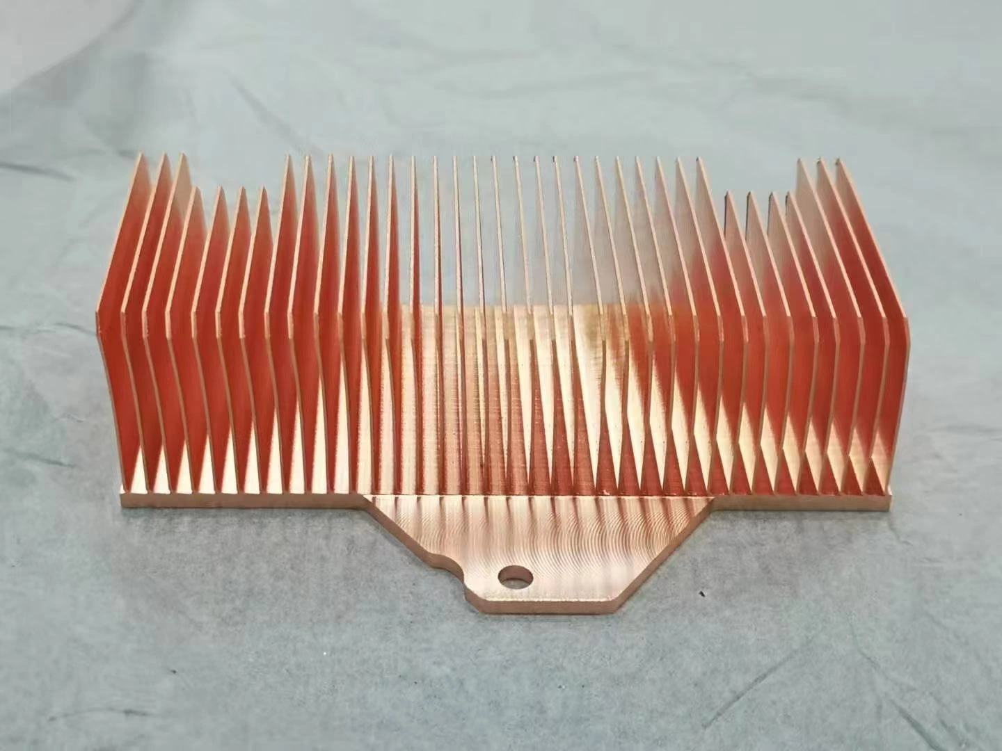
A reference part, with every number
Rather than quote ranges, here is one worked part. Not a customer's part — a rounded reference so the numbers can be checked against your own.
| Dimension | Value | What it means |
|---|---|---|
| Envelope | 150 × 100 × 15.00 mm | Also the size of the solid blank |
| Base thickness | 3.00 mm | Spreading path under the hot spot |
| Fin thickness | 0.30 mm | Middle of the copper working band |
| Fin height | 12.00 mm | Envelope minus base |
| Aspect ratio | 40:1 | Milling would stop at roughly 8:1 — a 1.50 mm fin |
| Pitch / air gap | 1.50 mm / 1.20 mm | 100 fins across the 150 mm side |
| Metal in the part | 81.0 cm³ — 36% of envelope | Base 45.0 cm³ + fins 36.0 cm³ |
| Weight, copper C11000 | 726 g | At 8.96 g/cm³ |
| Weight, aluminium 6063 | 219 g | 3.3× lighter, for 1.9× less conductivity |
| Surface area | 150 cm² → 2,550 cm² | The fins multiply it by 17 |
| Copper blank | 2,016 g | Two thirds of the bar leaves as chip |
That last row is the one nobody puts on a website. Skiving starts from a solid block the size of the whole envelope, so on a copper part the material line tracks the envelope, not the finished weight — 2,016 g of bar to ship 726 g of heat sink. Trimming a few millimetres off the envelope is worth more than trimming the fins.
Sizes that come up again and again
Skived copper heat sinks cluster around a handful of footprints, because they follow the devices underneath them — a module, a driver, a socket. These are the ones we build most often. If your part lands on or near one of these, say so in the enquiry: it shortens the quote and usually the lead time.
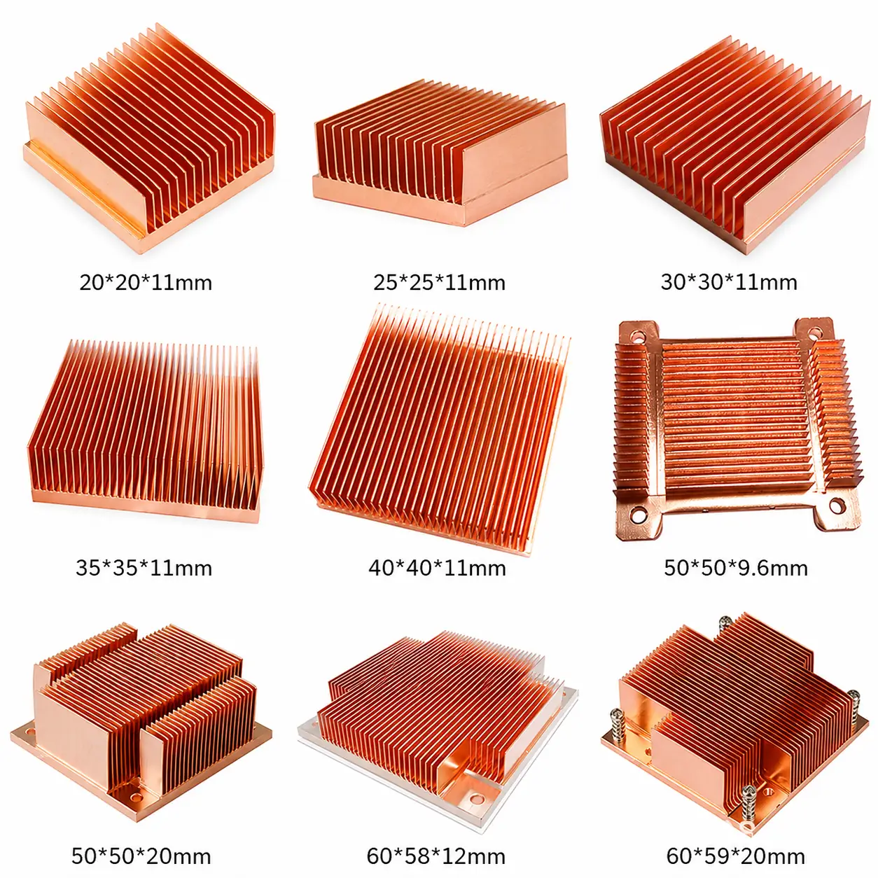
| Base | Overall height | Fin field | What it usually sits on |
|---|---|---|---|
| 20 × 20 mm | 11.00 mm | Full, edge to edge | Single driver IC, small SMD module |
| 25 × 25 mm | 11.00 mm | Full | DC-DC module, RF power device |
| 30 × 30 mm | 11.00 mm | Full | FPGA, SoC, camera module |
| 35 × 35 mm | 11.00 mm | Full, high density | Processor or laser diode carrier |
| 40 × 40 mm | 11.00 mm | Full, high density | Larger processor, power stage |
| 50 × 50 mm | 9.60 mm | Full, with mounting bracket | Board-mounted device with spring-clip retention |
| 50 × 50 mm | 20.00 mm | Segmented — channel through the middle | Two devices, or a duct passing through |
| 60 × 58 mm | 12.00 mm | Full, on a separate spreader plate | Mixed-metal build: copper fins, larger contact plate |
| 60 × 59 mm | 20.00 mm | Segmented, sprung captive screws | Socketed device needing even clamp load |
Read the three rows marked in white: segmented fields, spreader plates and captive spring screws are already normal work here, not special requests. Those are exactly the features that force a designer off a catalogue extrusion, and they are the reason most of these parts exist.
Which metals skive, and which refuse
| Metal | Conductivity | Skivable? | The reason |
|---|---|---|---|
| Copper C11000 (Cu-ETP) | ≈388 W/m·K | Yes — the reference | Ductile; the ribbon folds without cracking |
| Copper C10200 (OFC) | ≈390 W/m·K | Yes | Same behaviour, chosen where oxygen content matters |
| Aluminium 1050 | ≈229 W/m·K | Yes | Softest common aluminium — the best of the aluminiums here |
| Aluminium 6063 | ≈201 W/m·K | Yes | Works in the O and T4 tempers; T6 gets marginal |
| Copper C14500 (tellurium) | ≈355 W/m·K | No | Tellurium is added to break the chip — exactly what skiving must not do |
| Brass CuZn39Pb3 (CW614N) | ≈117 W/m·K | No | Lead breaks the chip, and the conductivity is worse than aluminium anyway |
| Aluminium 6061-T6 | ≈167 W/m·K | No — temper too hard | Fine for milled fins; the fin cracks at the fold |
| Aluminium 7075-T6 | ≈130 W/m·K | No | Harder still, and thermally a step down from 6061 |
| Stainless 304 | ≈16 W/m·K | No | Out on conductivity before process is even discussed |
Two things fall out of that table that are worth saying plainly. Brass has no business in a heat sink — it carries almost copper's mass at less than a third of copper's conductivity, which is worse than aluminium on both counts simultaneously. And if a drawing specifies 6061-T6 with 0.50 mm fins, the drawing contradicts itself: that alloy in that temper will not fold. Either the fin gets thicker, the alloy changes to 1050 or 6063, or the part becomes a bonded fin.
Reading a copper grade off someone else's standard
Half the skived fin enquiries we get name the copper in a standard other than the one above. A Japanese drawing says C1100, a Chinese mill certificate says T2, a European spec says Cu-ETP — all three are the same alloy this page calls C11000, electrolytic tough pitch copper at minimum 99.90% Cu. Send whichever designation your drawing carries; the table below is how we match it.
| Copper | US — UNS / ASTM | Europe — EN 13601 | Japan — JIS H3100 | China — GB/T 5231 |
|---|---|---|---|---|
| Tough pitch (ETP) — skives, the reference | C11000 | Cu-ETP / CW004A | C1100 | T2 |
| Oxygen-free (OF) — skives | C10200 | Cu-OF | C1020 | TU1 |
| Tellurium — does not skive | C14500 | CuTeP / CW118C | C1450 | — |
C1100 is the Japanese designation, not a Western one. The pair that gets confused with it is C11000 (UNS) and Cu-ETP / CW004A (EN) — one digit apart on paper, identical metal in the bar. The tellurium grade is the one to watch on this page: it has no GB number we can point to, Chinese mills quote it as C14500 directly, and whatever standard names it, it still will not skive — the tellurium is there to break the chip, and skiving needs the chip to survive.
Wave fins, two-sided fields, and fields that stop
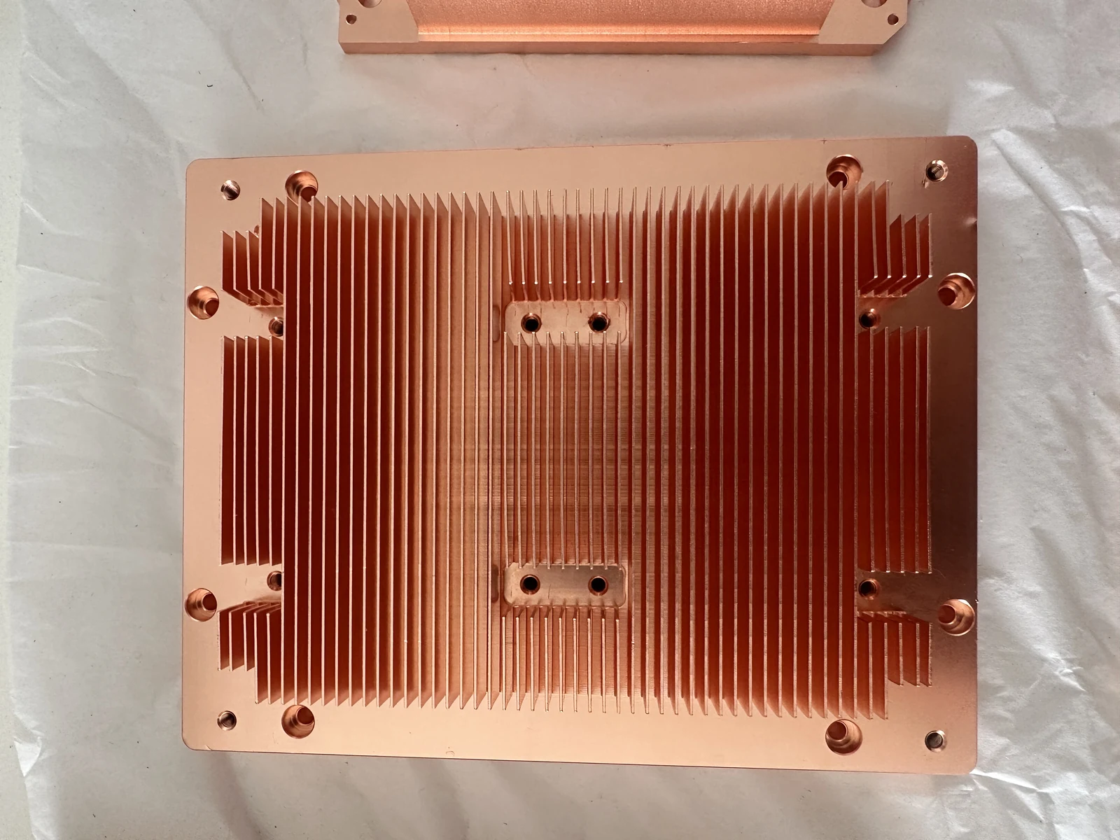
An extruded profile has one constant cross-section for its entire length. Every fin the same height, the field running edge to edge, nothing interrupting it. That is why extrusion is cheap, and it is exactly the boundary a skived or machined field steps over.
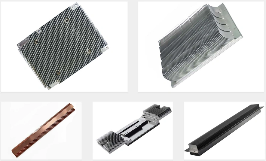
Wave fins
A wave or corrugated fin is deliberately not flat. As air travels along it, the thermal boundary layer keeps being disturbed instead of thickening steadily, so the same frontal area moves more heat. The price is pressure drop — which is why wave fins belong in ducted, fan-fed designs and are usually the wrong answer in natural convection, where you want the air to move freely and the fin count to come down instead.
Two-sided fin fields
Fins cut from both faces of the same base. No single extrusion die can produce it, because a die produces one section. Typical use is a plate sitting between two heat sources, or a duct where air passes on both sides of the plate.
Segmented fields and stepped heights
Fin fields that break to let a fastener through, that stop short of a machined pad, or that step between heights across one base. On a catalogue profile the designer has to move the screws outboard of the fin field and lose footprint. On a cut field the screws land wherever the enclosure needs them.
Twenty pieces, not five hundred
Here is the single most common message that arrives on this page, almost word for word: "I need 20 pieces with 0.4 mm fins and every skiving shop I contact wants a 500-piece minimum."
That minimum is real, and it is not about your fin. Skiving needs a blade and a fixture ground for your specific pitch, and that cost does not spread across twenty pieces. So below roughly fifty pieces we do not skive — we build the same part as a bonded fin: rolled sheet of 0.30 to 1.00 mm set into slots machined in the base, then soldered or brazed. Same fin density, no tooling, from 1 piece.
The honest difference is a joint at the fin root. A skived fin is monolithic — metal runs continuously from base into fin — while a bonded fin has an interface there that adds a little contact resistance. On most parts that costs less than the tooling would, and above roughly five hundred pieces the arithmetic flips and skiving wins. We tell you where your crossover sits instead of pushing one route.
| What you need | In the catalogue? | What we do about it |
|---|---|---|
| Standard skived heat sink in a common footprint | Yes — several thermal houses stock them | Buy it off the shelf — it will beat our price. Or ask us: if the catalogue part fits, we say so instead of quoting. |
| CPU cooler, GPU cooler, anything for a PC build | Yes — a whole retail industry | Not our market, and retail pricing will always win there. |
| 0.30 mm copper fins, quantity 20 | No — minimums start around 500 | Bonded fin: same density, no tooling, from 1 piece |
| Fin field that must open around mounting screws | No — a die makes one constant section | Segmented field cut to your fastener layout |
| Fins on both faces of one base | No | Cut both faces on a machined base |
| Wave or corrugated fin for a duct | Rarely, and never in your dimensions | Formed or cut to the wave pitch your pressure budget allows |
| Copper base carrying aluminium fins | No — one die, one metal | Bonded fin makes mixed-metal builds straightforward |
| 50,000 skived pieces a year, standard section | Effectively yes | A dedicated skiving line will beat us. Go there. |
What your drawing needs before we can quote
- Fin thickness, height and pitch. These three decide the process before anything else does.
- The specific alloy — C11000 and C14500 are both "copper" and only one of them skives.
- Flatness of the contact face. On a thermal interface this is the dimension that sets the price; a base that rocks throws away performance no fin design recovers.
- The finish. Nickel plating adds a layer far less conductive than copper — on the contact face specify it as thin as possible, or mask it off. Copper cannot be anodised at all.
Missing one of the four? We ask before quoting rather than assuming a value and pricing the wrong part. A STEP file, a dimensioned drawing, a hand sketch or the old part itself are all normal starting points, and a sketch gets redrawn into CAD at no charge before anything is cut.
A real job of this kind: A Special-Profile Heat Sink in 6061, Small Quantity — a special-profile 6061 heat sink in a small quantity, cut by wire EDM because an extrusion die would have cost more than the order.
Frequently Asked Questions
In copper, 0.20 mm is reachable and 0.30 to 0.50 mm is the ordinary working band. The limit is not the blade — it is whether the fin survives handling, cleaning and packing afterwards. A 0.20 mm copper fin 15.00 mm tall will bend if a thumb lands on it, so unless the design needs that density we steer to 0.30 or 0.40 mm, which costs almost nothing in thermal performance and survives the trip. In aluminium 1050 and 6063 the practical floor is a little higher, around 0.40 mm.
Because of which piece of metal the tool is pushing on. When you mill a fin field, the fin is what is left standing after the slot beside it is cut, so the finished fin takes the full side load of the cutter — thin and tall, it chatters, leans and tears. When you skive, the fin is the metal being removed: the blade runs almost parallel to the surface, lifts a continuous ribbon and folds it upright, still joined at the root. Nothing ever pushes sideways on the finished fin. That single difference is worth a factor of five in aspect ratio.
Skivable: copper C11000 (Cu-ETP) at about 388 W/m·K, copper C10200 OFC at about 390 W/m·K, aluminium 1050 at about 229 W/m·K and aluminium 6063 at about 201 W/m·K. Not skivable: tellurium copper C14500 and leaded brass CuZn39Pb3, because tellurium and lead are added precisely to break the chip and skiving needs the opposite, one continuous ribbon that survives the fold; aluminium 6061-T6 and 7075-T6, too hard in that temper; stainless 304 at about 16 W/m·K, which is ruled out on conductivity before the process question even arises. The awkward part of that list is that the easiest alloys to machine are exactly the ones that cannot be skived.
Yes to both, and they are the geometries a catalogue profile cannot reach. A wave or corrugated fin is deliberately not flat, so the boundary layer keeps being broken up along the fin length and the same frontal area moves more heat in forced air — at the cost of pressure drop, which is why it belongs in ducted and fan-fed designs rather than natural convection. A two-sided fin field is exactly what it sounds like: fins cut from both faces of one base, which no single extrusion die can produce because a die only makes one constant section. We also cut segmented fields with clearance opened around fasteners, and fields that step between heights on one base.
That minimum is about the blade and the fixture, both ground for your specific fin pitch, and neither cost spreads over 20 pieces. Below roughly 50 pieces we propose bonded fin instead: 0.30 to 1.00 mm rolled sheet set into slots machined in the base, then soldered or brazed. Same fin density, no tooling, from 1 piece. The honest difference is a joint at the fin root that adds a little contact resistance where a skived fin is monolithic. Above roughly 500 pieces skiving usually wins on price and on that joint, and we will tell you where your crossover falls.
More than the finished weight suggests, and this is the part that surprises buyers pricing their first one. Skiving starts from a solid block the size of the full envelope. On the reference part here — 150 x 100 x 15 mm with 100 fins of 0.30 mm — the finished piece holds 81.0 cm3 of metal, 726 g in copper, but the blank is the whole 225 cm3 envelope, about 2016 g. Roughly two thirds of the bar leaves as chip. So the material line on a copper skived part tracks the envelope, not the part weight, and shrinking the envelope by a few millimetres saves real money.
Fin thickness, fin height and pitch, because those three set the process before anything else does. The specific alloy, not just copper or aluminium — C11000 and C14500 are both copper and only one of them skives. Flatness of the contact face, which on a thermal interface is the dimension that sets the price. And the finish, keeping in mind that nickel plating adds a layer much less conductive than copper, so on the contact face specify it thin or mask it off. Copper cannot be anodised at all. Send a STEP file, a dimensioned drawing or a hand sketch — all three are normal here.
Related: all fin processes compared · extruded heat sinks · machined aluminum heat sinks · copper machining · cold plates · order from a sketch · low-MOQ parts
Get a Free Quote
Send fin thickness, height and pitch, the base footprint and the quantity. We reply within 12 hours — including when the honest answer is "buy the catalogue part".
// Route by quantity
1–50
Bonded fin
No blade, no fixture
50–500
Either
Decided on the part
500+
Skived
Monolithic fin root
- →Wave, two-sided and segmented fin fields all cut here
- →No CAD? A sketch with pitch and height is enough
Response within 12h · Drawings kept confidential